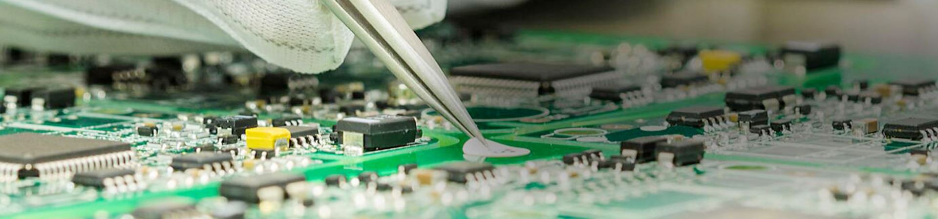
can be divided into several types based on the number and complexity of circuit layers, including 1 Step, 2 Stepr, and 3 Step. The main differences lie in the layer structure, manufacturing process, and applicable scenarios. The following will explain the technical characteristics and application fields.
1 Step HDI circuit board
Process flow: The 1 Step HDI PCB adopts a single layer manufacturing process, and the process and technology are relatively easy to control.
(Usually a single-sided or double-sided structure, containing only one circuit layer, with interlayer connection achieved through a single micro hole (laser drilling) process)
For example, simple circuit modules for smartphones, Bluetooth earphones, and other consumer electronics products often use this type of design, which can meet basic functions while controlling production costs. More suitable for large-scale production.

2 Step HDI circuit board
Multiple pressing and punching processes are required for 2 Step HDI PCBs, which require two or more layering techniques and involve multiple pressing and laser punching processes. Compared to 1 Step, it has a higher wiring density, supports
Typical applications: including high-performance devices such as the main control board and server motherboard of 5G communication base stations. These scenarios require a balance between signal integrity and heat dissipation capabilities. The multi-layer structure of the 2 Step HDI board can effectively optimize electromagnetic interference problems.

3 Step HDI circuit board
Highest technology: The 3 Step HDI board is the most complex type, consisting of three or more circuit layers, and requires multiple lamination and high-precision laser drilling to achieve interlayer interconnection (such as sequential lamination process).
This type of circuit board is mainly used in cutting-edge fields such as satellite communication equipment and military radar systems. Its multi-layer stacking design can support large capacity data processing while adapting to harsh conditions such as high temperature and high vibration.

In summary, from a technical perspective, the key to hierarchical division lies in the performance improvement brought about by increasing the number of layers: the 1 Step focuses on cost control, the 2 Step strengthens high-frequency signal processing, and the 3 Step pursues ultimate performance.The application scenarios are upgrading from consumer electronics to industrial and military fields, with high layer. Of course, the difficulty and cost of manufacturing processes are also increasing exponentially.
Uniwell Circuits carefully selects superior materials with excellent electrical performance, durability, and environmental friendliness, and has no special requirements for order design. No matter how creative or complex your 1-4 Step HDI sample customization is, feel free to contact Uniwell Circuit's professional engineers. We will be dedicated to serving you.
What is the difference between HDI and FR4?
What is better than FR4?